Äîêóìåíòàöèÿ è îïèñàíèÿ www.docs.chipfind.ru
1
LTC1483
Ultra-Low Power RS485 Low EMI
Transceiver with Shutdown
S
FEATURE
D
U
ESCRIPTIO
The LTC
®
1483 is an ultra-low power differential line trans-
ceiver designed for data transmission standard RS485
applications with extended common-mode range ( 7V to
12V). It will also meet the requirements of RS422. The
LTC1483 features output drivers with controlled slew rate,
decreasing the EMI radiated from the RS485 lines, and
improving signal fidelity with misterminated lines. The
CMOS design offers significant power savings over its
bipolar counterparts without sacrificing ruggedness against
overload or ESD damage. Typical quiescent current is only
80
µ
A while operating and less than 1
µ
A in shutdown.
The driver and receiver feature three-state outputs, with
the driver outputs maintaining high impedance over the
entire common-mode range. Excessive power dissipation
caused by bus contention or faults is prevented by a
thermal shutdown circuit which forces the driver outputs
into a high impedance state. The receiver has a fail-safe
feature which guarantees a high output state when the
inputs are left open. I/O pins are protected against multiple
ESD strikes of over
±
10kV.
The LTC1483 is fully specified over the commercial and
extended industrial temperature range and is available in
8-pin DIP and SO packages.
s
Low Power: I
CC
= 120
µ
A Max with Driver Disabled
s
I
CC
= 500
µ
A Max with Driver Enabled, No Load
s
1
µ
A Quiescent Current in Shutdown Mode
s
Controlled Slew Rate Driver for Reduced EMI
s
Single 5V Supply
s
Drivers/Receivers Have
±
10kV ESD Protection
s
7V to 12V Common-Mode Range Permits
±
7V
Ground Difference Between Devices on the Data Line
s
Thermal Shutdown Protection
s
Power Up/Down Glitch-Free Driver Outputs Permit
Live Insertion or Removal of Transceiver
s
Driver Maintains High Impedance in Three-State
or with the Power Off
s
Up to 32 Transceivers on the Bus
s
Pin Compatible with the LTC485
s
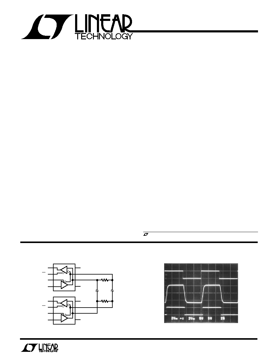
Battery-Powered RS485/RS422 Applications
s
Low Power RS485/RS422 Transceiver
s
Level Translator
U
S
A
O
PPLICATI
U
A
O
PPLICATI
TYPICAL
V
CC1
GND1
R
RO1
RE1
DE1
DI1
D
V
CC2
GND2
R
RO2
RE2
DE2
DI2
D
R
TERM
R
TERM
LTC1483 · TA01
RO
A B
DI
1483 TA02
, LTC and LT are registered trademarks of Linear Technology Corporation.
2
LTC1483
SYMBOL
PARAMETER
CONDITIONS
MIN
TYP
MAX
UNITS
V
OD1
Differential Driver Output Voltage (Unloaded)
I
O
= 0
q
5
V
V
OD2
Differential Driver Output Voltage (with Load)
R = 50
(RS422)
q
2
V
R = 27
(RS485), Figure 1
q
1.5
5
V
V
OD
Change in Magnitude of Driver Differential Output
R = 27
or R = 50
, Figure 1
q
0.2
V
Voltage for Complementary Output States
V
OC
Driver Common-Mode Output Voltage
R = 27
or R = 50
, Figure 1
q
3
V
V
OC
Change in Magnitude of Driver Common-Mode
R = 27
or R = 50
, Figure 1
q
0.2
V
Output Voltage for Complementary Output States
V
IH
Input High Voltage
DE, DI, RE
q
2
V
V
IL
Input Low Voltage
DE, DI, RE
q
0.8
V
I
IN1
Input Current
DE, DI, RE
q
±
2
µ
A
I
IN2
Input Current (A, B)
DE = 0, V
CC
= 0V or 5.25V, V
IN
= 12V
q
1.0
mA
DE = 0, V
CC
= 0V or 5.25V, V
IN
= 7V
q
0.8
mA
V
TH
Differential Input Threshold Voltage for Receiver
7V
V
CM
12V
q
0.2
0.2
V
V
TH
Receiver Input Hysteresis
V
CM
= 0V
q
45
mV
V
OH
Receiver Output High Voltage
I
O
= 4mA, V
ID
= 200mV
q
3.5
V
V
OL
Receiver Output Low Voltage
I
O
= 4mA, V
ID
= 200mV
q
0.4
V
I
OZR
Three-State (High Impedance) Output
V
CC
= Max, 0.4V
V
O
2.4V
q
±
1
µ
A
Current at Receiver
R
IN
Receiver Input Resistance
7V
V
CM
12V
q
12
25
k
I
CC
Supply Current
No Load, Output Enabled
q
300
500
µ
A
No Load, Output Disabled
q
80
120
µ
A
I
SHDN
Supply Current in Shutdown Mode
DE = 0, RE = V
CC
1
10
µ
A
I
OSD1
Driver Short-Circuit Current, V
OUT
= HIGH
7V
V
O
12V
q
35
250
mA
I
OSD2
Driver Short-Circuit Current, V
OUT
= LOW
7V
V
O
12V
q
35
250
mA
I
OSR
Receiver Short-Circuit Current
0V
V
O
V
CC
q
7
85
mA
A
U
G
W
A
W
U
W
A
R
BSOLUTE
XI
TI
S
W
U
U
PACKAGE/ORDER I FOR ATIO
ORDER PART
NUMBER
LTC1483CN8
LTC1483IN8
LTC1483CS8
LTC1483IS8
(Note 1)
Supply Voltage (V
CC
) .............................................. 12V
Control Input Voltage ..................... 0.5V to V
CC
+ 0.5V
Driver Input Voltage ....................... 0.5V to V
CC
+ 0.5V
Driver Output Voltage ...........................................
±
14V
Receiver Input Voltage ..........................................
±
14V
Receiver Output Voltage ................ 0.5V to V
CC
+ 0.5V
Operating Temperature Range
LTC1483C ........................................ 0
°
C
T
A
70
°
C
LTC1483I .................................... 40
°
C
T
A
85
°
C
Lead Temperature (Soldering, 10 sec) ................. 300
°
C
T
JMAX
= 125
°
C,
JA
= 130
°
C/ W (N8)
T
JMAX
= 125
°
C,
JA
= 150
°
C/ W (S8)
S8 PART MARKING
1483
1483I
Consult factory for Military grade parts.
ELECTRICAL C
C
HARA TERISTICS
V
CC
= 5V, (Notes 2, 3) unless otherwise noted.
1
2
3
4
8
7
6
5
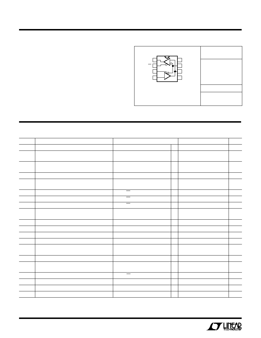
TOP VIEW
V
CC
B
A
GND
N8 PACKAGE
8-LEAD PDIP
S8 PACKAGE
8-LEAD PLASTIC SO
R
D
RO
RE
DE
DI
3
LTC1483
V
CC
= 5V, (Notes 2, 3) unless otherwise noted.
SWITCHI G CHARACTERISTICS
U
Note 2: All currents into device pins are positive; all currents out ot device
pins are negative. All voltages are referenced to device ground unless
otherwise specified.
Note 3: All typicals are given for V
CC
= 5V and T
A
= 25
°
C.
The
q
denotes specifications which apply over the full operating
temperature range.
Note 1: Absolute maximum ratings are those beyond which the safety of
the device cannot be guaranteed.
Supply Current vs Temperature
Receiver
t
PLH
t
PHL
vs
Temperature
TEMPERATURE (
°
C)
50
14
12
10
8
6
4
2
0
25
75
1483 G02
25
0
50
100
125
t
PLH
t
PHL
(ns)
Driver Differential Output Voltage
vs Output Current
OUTPUT VOLTAGE (V)
0
70
60
50
40
30
20
10
0
3
1483 G03
1
2
4
5
OUTPUT CURRENT (mA)
T
A
= 25
°
C
TYPICAL PERFOR
M
A
N
CE CHARACTERISTICS
U
W
TEMPERATURE (
°
C)
50
SUPPLY CURRENT (
µ
A)
50
350
300
250
200
150
100
50
0
1483 G01
0
25
25
75
125
175
150
100
DRIVER ENABLED
DRIVER DISABLED
THERMAL SHUTDOWN
WITH DRIVER ENABLED
LTC1483
SYMBOL
PARAMETER
CONDITIONS
MIN
TYP
MAX
UNITS
t
PLH
Driver Input to Output
R
DIFF
= 54
, C
L1
= C
L2
= 100pF,
q
150
1200
ns
t
PHL
Driver Input to Output
q
150
1200
ns
t
SKEW
Driver Output to Output
q
100
600
ns
t
r
, t
f
Driver Rise or Fall Time
q
150
1200
ns
t
ZH
Driver Enable to Output High
C
L
= 100pF (Figures 4, 6), S2 Closed
q
100
1500
ns
t
ZL
Driver Enable to Output Low
C
L
= 100pF (Figures 4, 6), S1 Closed
q
100
1500
ns
t
LZ
Driver Disable Time from Low
C
L
= 15pF (Figures 4, 6), S1 Closed
q
150
1500
ns
t
HZ
Driver Disable Time from High
C
L
= 15pF (Figures 4, 6), S2 Closed
q
150
1500
ns
t
PLH
Receiver Input to Output
R
DIFF
= 54
, C
L1
= C
L2
= 100pF,
q
30
140
200
ns
t
PHL
Receiver Input to Output
q
30
140
200
ns
t
SKD
t
PLH
t
PHL
Differential Receiver Skew
q
13
ns
t
ZL
Receiver Enable to Output Low
C
RL
= 15pF (Figures 2, 8), S1 Closed
q
20
50
ns
t
ZH
Receiver Enable to Output High
C
RL
= 15pF (Figures 2, 8), S2 Closed
q
20
50
ns
t
LZ
Receiver Disable from Low
C
RL
= 15pF (Figures 2, 8), S1 Closed
q
20
50
ns
t
HZ
Receiver Disable from High
C
RL
= 15pF (Figures 2, 8), S2 Closed
q
20
50
ns
f
MAX
Maximum Data Rate
q
250
kbits/s
t
SHDN
Time to Shutdown
DE = 0, RE =
q
50
200
600
ns
t
ZH(SHDN)
Driver Enable from Shutdown to Output High
C
L
= 100pF (Figures 4, 6), S2 Closed
q
2000
ns
t
ZL(SHDN)
Driver Enable from Shutdown to Output Low
C
L
= 100pF (Figures 4, 6), S1 Closed
q
2000
ns
t
ZH(SHDN)
Receiver Enable from Shutdown to Output High
C
L
= 15pF (Figures 2, 8), S2 Closed
q
3500
ns
t
ZL(SHDN)
Receiver Enable from Shutdown to Output Low
C
L
= 15pF (Figures 2, 8), S1 Closed
q
3500
ns
(Figures 3, 5)
(Figures 3, 7)
4
LTC1483
TYPICAL PERFOR
M
A
N
CE CHARACTERISTICS
U
W
Driver Differential Output Voltage
vs Temperature
TEMPERATURE (
°
C)
50
DIFFERENTIAL VOLTAGE (V)
2.5
2.4
2.3
2.2
2.1
2.0
1.9
1.8
1.7
1.6
1.5
0
50
75
1483 G04
25
25
100
125
R
L
= 54
Driver Output High Voltage
vs Output Current
OUTPUT VOLTAGE (V)
0
OUTPUT CURRENT (mA)
2
4
5
0
10
20
30
40
50
60
70
80
90
1483 G06
1
3
T
A
= 25
°
C
PI
N
FU
N
CTIO
N
S
U
U
U
DI (Pin 4): Driver Input. If the driver outputs are enabled
(DE high) then a low on DI forces the outputs A low and B
high. A high on DI with the driver outputs enabled will force
A high and B low.
GND (Pin 5): Ground.
A (Pin 6): Driver Output/Receiver Input.
B (Pin 7): Driver Output/Receiver Input.
V
CC
(Pin 8): Positive Supply. 4.75V < V
CC
< 5.25V.
RO (Pin 1): Receiver Output. If the receiver output is
enabled (RE low), then if A > B by 200mV, RO will be high.
If A < B by 200mV, then RO will be low.
RE (Pin 2): Receiver Output Enable. A low enables the
receiver output, RO. A high input forces the receiver
output into a high impedance state.
DE (Pin 3): Driver Outputs Enable. A high on DE enables
the driver output. A, B and the chip will function as a line
driver. A low input will force the driver outputs into a high
impedance state and the chip will function as a line
receiver. If RE is high and DE is low, the part will enter a low
power (1
µ
A) shutdown state.
FU CTIO TABLES
U
U
LTC1483 Transmitting
INPUTS
OUTPUTS
RE
DE
DI
B
A
X
1
1
0
1
X
1
0
1
0
0
0
X
Z
Z
1
0
X
Z*
Z*
*Shutdown mode for LTC1483
LTC1483 Receiving
INPUTS
OUTPUTS
RE
DE
A B
RO
0
0
0.2V
1
0
0
0.2V
0
0
0
Inputs Open
1
1
0
X
Z*
*Shutdown mode for LTC1483
OUTPUT VOLTAGE
0
70
60
50
40
30
20
10
0
3
1483 G05
1
2
4
OUTPUT CURRENT (mA)
T
A
= 25
°
C
Driver Output Low Voltage
vs Output Current
5
LTC1483
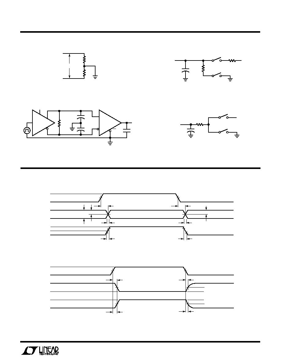
TEST CIRCUITS
SWITCHI G TI E WAVEFOR S
U
W
W
3V
DE
A
B
DI
R
DIFF
C
L1
C
L2
RO
15pF
A
B
RE
LTC1483 · F03
Figure 3. Driver/ Receiver Timing Test Circuit
Figure 4. Driver Timing Test Load
OUTPUT
UNDER TEST
C
L
S1
S2
V
CC
500
LTC1483 · F04
V
OD
A
B
R
R
V
OC
LTC1483 · F01
RECEIVER
OUTPUT
C
RL
1k
S1
S2
TEST POINT
V
CC
1k
LTC1483 · F02
Figure 1. Driver DC Test Load
Figure 2. Receiver Timing Test Load
Figure 6. Driver Enable and Disable Times
1.5V
2.3V
2.3V
t
ZH(SHDN)
,
t
ZH
t
ZL(SHDN)
,
t
ZL
1.5V
t
LZ
0.5V
0.5V
t
HZ
OUTPUT NORMALLY LOW
OUTPUT NORMALLY HIGH
3V
0V
DE
5V
V
OL
V
OH
0V
A, B
A, B
LTC1483 · F06
t
r
10ns, t
f
10ns
Figure 5. Driver Propagation Delays
DI
3V
1.5V
t
PLH
t
r
t
SKEW
1/2 V
O
V
O
t
r
10ns, t
f
10ns
90%
10%
0V
B
A
V
O
V
O
0V
90%
1.5V
t
PHL
t
SKEW
1/2 V
O
10%
t
f
V
DIFF
= V(A) V(B)
LTC1483 · F05